
While experimental data and methods are commonly reported as “best outcome” figure of merits, the systematic process parameters are often neglected or buried in hard-to-access lab books and similar sources. This complicates and prolongs process optimization, especially when different printing and post-processing steps need to be combined for a specific application. The project ReCIPE aimed at setting up a broad open database on process parameters and connected outcomes to eventually support the wider academic and industry-based community.
The field of printed electronics is striving to develop novel applications in various research areas with the help of additive manufacturing processes and more sustainable techniques for inexpensive and mass available devices, in particular on flexible substrates (e.g. for sensing or biomedical applications). One of the key advantages in printable electronics is the wide range of materials that can be used in many different printing methods. On the other hand, the same diversity in materials and methods bring along the challenge of finding the ideal choice in the combination of material, method and accompanying processing parameters for a given application or target device.There is a need to find a way to exchange this information on methods, process chains and sample treatments as well as the obtained device performances in a standardized and openly accessible manner.
To adress this need, we proposed “ReCIPE – Metadata Framework and Rich Provenance Tracking system for Conductive Inks in Printed Electronics” as part of the NFDI4Ing Seed Fund programme 2022. The main goal of ReCIPE was to establish a data and metadata structure for the use case of conductive inks. Conductive ink, based on metallic inks, can be seen as being a pressing topic in the field of printed electronics, since the conductivity obtained from printable conductive inks after processing often remains behind expectation.
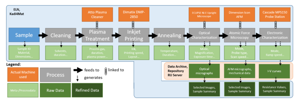
After intense research into alternatives we eventually decided on Kadi4Mat as a platform. Next, regular interviews with members of different research groups working on printed electronics were scheduled. The goal was to survey the details of process chains and machines involved in them, as well as which parameters were typically recorded and what experimental data was derived in the end. This data was then modelled into actual process descriptions and implemented into templates and flexible process chains. Additionally, regular meetings with the lead developers of Kadi4Mat were installed and proved to be extremely helpful in implementing the developed ontology and modelling of the identified process chains into the Kadi4Mat platform. As result of our efforts, we successfully implemented a model process for printing of metallic nanoparticle inks that was filled with pilot experiments (Fig. 1).
As of February 2023, we have recorded complete data sets of fabrication and characterization for inkjet printing of interconnects with Au, Ag and Pt nanoparticle formulations under different process parameters in regard to morphology and conductivity. This is a strong basis for the envisioned database, as now additional experiments with an even broader parameter space as well as new ink formulations can quickly be added. The platform is now open for use in collaborations outside the KIT (in particular in projects in the framework of the Karlsruhe Nano Micro Facility).
The results of our seed project are subject to a publication in preparation that we plan to submit once a critical mass of experiment sets open to the general public was generated. Overall, the seed fund project ReCIPE did not only allow us to install the basis for a process and result database in regard to metallic interconnect fabrication in printed electronics, but also gave a boost to the development in digital RDM and ELN use in a much broader context.
PD Dr. Dr. Michael Hirtz
Karlsruhe Institute of Technology (KIT)
Institute of Nanotechnology (INT) & Karlsruhe Nano Micro Facility (KNMFi)
This text is based on the final report delivered to the NFDI4Ing steering committee.
Edited by Thorsten Schwetje